- 您现在的位置:买卖IC网 > Sheet目录3887 > PIC16F872T-E/SO (Microchip Technology)IC MCU CMOS 20MHZ 2K FLSH 28SOIC
102
8048C–AVR–02/12
ATtiny43U
14. USI – Universal Serial Interface
14.1
Features
Two-wire Synchronous Data Transfer (Master or Slave)
Three-wire Synchronous Data Transfer (Master or Slave)
Data Received Interrupt
Wakeup from Idle Mode
In Two-wire Mode: Wake-up from All Sleep Modes, Including Power-down Mode
Two-wire Start Condition Detector with Interrupt Capability
14.2
Overview
The Universal Serial Interface (USI), provides the basic hardware resources needed for serial
communication. Combined with a minimum of control software, the USI allows significantly
higher transfer rates and uses less code space than solutions based on software only. Interrupts
are included to minimize the processor load.
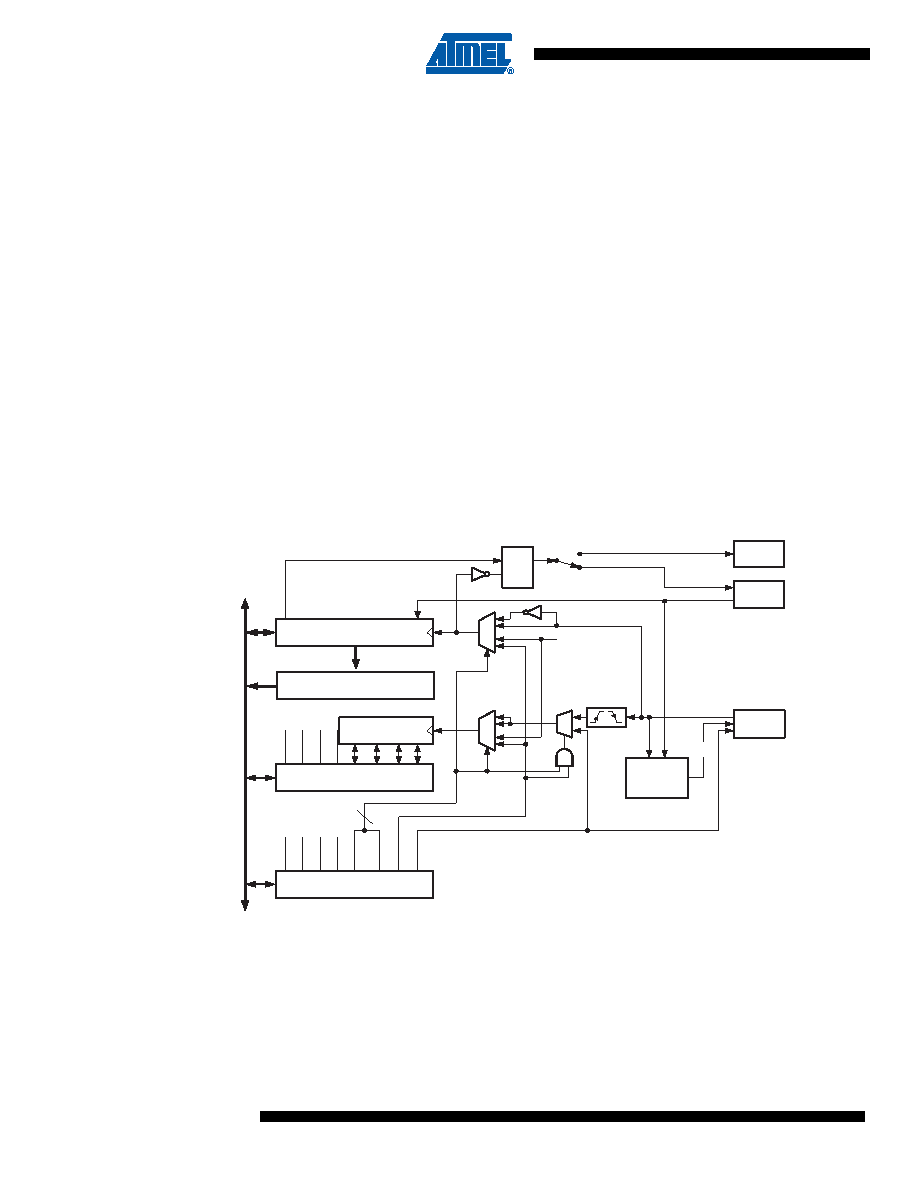
A simplified block diagram of the USI is shown in Figure 14-1 on page 102. For actual placement
of I/O pins, refer to “Pinout of ATtiny43U” on page 2. CPU accessible I/O Registers, including I/O
bits and I/O pins, are shown in bold. The device-specific I/O Register and bit locations are listed
Figure 14-1. Universal Serial Interface, Block Diagram
The 8-bit USI Data Register (USIDR) contains the incoming and outgoing data. It is directly
accessible via the data bus but a copy of the contents is also placed in the USI Buffer Register
(USIBR) where it can be retrieved later. If reading the USI Data Register directly, the register
must be read as quickly as possible to ensure that no data is lost.
The most significant bit of the USI Data Register is connected to one of two output pins (depend-
ing on the mode configuration, see Table 14-1 on page 110). There is a transparent latch
between the output of the USI Data Register and the output pin, which delays the change of data
DATA
BUS
USIPF
USITC
USICLK
USICS0
USICS1
USIOIF
USIOIE
USIDC
USISIF
USIWM0
USIWM1
USISIE
Bit7
Two-wire Clock
Control Unit
DO
(Output only)
DI/SDA
(Input/Open Drain)
USCK/SCL
(Input/Open Drain)
4-bit Counter
USIDR
USISR
DQ
LE
USICR
CLOCK
HOLD
TIM0 COMP
Bit0
[1]
3
0
1
2
3
0
1
2
0
1
2
USIDB
发布紧急采购,3分钟左右您将得到回复。
相关PDF资料
PIC16F727-E/P
IC PIC MCU FLASH 8KX14 40-DIP
PIC16F871T-E/PT
IC MCU CMOS 20MHZ 2K FLSH 44TQFP
PIC16F871T-E/L
IC MCU CMOS 20MHZ 2K FLSH 44PLCC
PIC16F871-E/PT
IC MCU CMOS 20MHZ 2K FLSH 44TQFP
PIC16F871-E/L
IC MCU CMOS 20MHZ 2K FLSH 44PLCC
PIC16F870T-E/SS
IC MCU CMOS 20MHZ 2K FLSH 28SSOP
PIC16F870T-E/SO
IC MCU CMOS 20MHZ 2K FLSH 28SOIC
PIC16F84AT-20E/SS
IC MCU CMOS 20MHZ 1K FLSH 20SSOP
相关代理商/技术参数
PIC16F872T-E/SS
功能描述:8位微控制器 -MCU 3.5KB 128 RAM 22 I/O RoHS:否 制造商:Silicon Labs 核心:8051 处理器系列:C8051F39x 数据总线宽度:8 bit 最大时钟频率:50 MHz 程序存储器大小:16 KB 数据 RAM 大小:1 KB 片上 ADC:Yes 工作电源电压:1.8 V to 3.6 V 工作温度范围:- 40 C to + 105 C 封装 / 箱体:QFN-20 安装风格:SMD/SMT
PIC16F872T-I/SO
功能描述:8位微控制器 -MCU 3.5KB 128 RAM 22 I/O RoHS:否 制造商:Silicon Labs 核心:8051 处理器系列:C8051F39x 数据总线宽度:8 bit 最大时钟频率:50 MHz 程序存储器大小:16 KB 数据 RAM 大小:1 KB 片上 ADC:Yes 工作电源电压:1.8 V to 3.6 V 工作温度范围:- 40 C to + 105 C 封装 / 箱体:QFN-20 安装风格:SMD/SMT
PIC16F872T-I/SS
功能描述:8位微控制器 -MCU 3.5KB 128 RAM 22 I/O RoHS:否 制造商:Silicon Labs 核心:8051 处理器系列:C8051F39x 数据总线宽度:8 bit 最大时钟频率:50 MHz 程序存储器大小:16 KB 数据 RAM 大小:1 KB 片上 ADC:Yes 工作电源电压:1.8 V to 3.6 V 工作温度范围:- 40 C to + 105 C 封装 / 箱体:QFN-20 安装风格:SMD/SMT
PIC16F872T-I/SS033
制造商:Microchip Technology Inc 功能描述:
PIC16F873-04/SO
功能描述:8位微控制器 -MCU 7KB 192 RAM 22 I/O RoHS:否 制造商:Silicon Labs 核心:8051 处理器系列:C8051F39x 数据总线宽度:8 bit 最大时钟频率:50 MHz 程序存储器大小:16 KB 数据 RAM 大小:1 KB 片上 ADC:Yes 工作电源电压:1.8 V to 3.6 V 工作温度范围:- 40 C to + 105 C 封装 / 箱体:QFN-20 安装风格:SMD/SMT
PIC16F873-04/SO
制造商:Microchip Technology Inc 功能描述:8BIT FLASH MCU SMD 16F873 SOIC28
PIC16F873-04/SP
功能描述:8位微控制器 -MCU 7KB 192 RAM 22 I/O RoHS:否 制造商:Silicon Labs 核心:8051 处理器系列:C8051F39x 数据总线宽度:8 bit 最大时钟频率:50 MHz 程序存储器大小:16 KB 数据 RAM 大小:1 KB 片上 ADC:Yes 工作电源电压:1.8 V to 3.6 V 工作温度范围:- 40 C to + 105 C 封装 / 箱体:QFN-20 安装风格:SMD/SMT
PIC16F873-04/SP
制造商:Microchip Technology Inc 功能描述:IC 8BIT FLASH MCU 16F873 SDIL28